

A bare through hole plated PCB for the Soundtronics Voltage Controlled Attack, Decay, Sustain, Release 3310 Envelope Generator.
The 'VC ADSR 3310' is an enhanced version of our 'ADSR 3310' envelope generator and is also based on the AS3310 chip with the following features:
- 1mS to 30 second Attack, Decay, and Release times.
- Trigger input for AR envelopes, also re-triggers attack phase if used in conjunction with the gate input
- Supply voltage +/- 12V as standard, change 5 resistors for +/- 15V operation
- Range switch offers finer adjustment for short timing periods
- Comparator on gate input making it suitable for gate pulses >2.5V
- Manual gate switch
- Twin ADSR outputs
- Individual voltage control inputs for the attack, decay and release timings + the sustain level
- Common voltage control input for the ADR timings that change all timings simultaneously
- Shape control pots for the attack, decay and release phases that allow exponential, linear and logarithmic shaps
- PCB suitable for 4 types of power supply connector - Soundtronics, Eurorack, Dotcom and MOTM
- Full 10V swing on ADSR output
- Optional JST leads for all connections although you can hardwire if you prefer
- Optional jack socket PCB 7210-733 and pot PCBs 7210-703 & 7210-704 simplifies wiring
For circuit schematic and PCB layout, see the 'Downloads' tab. See the 'Build Guide' tab for assembly instructions. See below for oscilloscope images of various envelopes.
As builders have differing preferences and build formats, the parts list below excludes knobs, JST sockets, 1/4" jack sockets and panels all of which are available from Soundtronics. See the ADSR 3310 main page here for further related products.
| Qty Reqd. | Description | Value | Designators | ST part No. |
| 1 | 33nF 2.5mm X7R Dielectric Radial Ceramic Capacitor | 33nF | C9 | 2069-070 |
| 3 | 300R 0.25W 1% Metal Film Resistor | 300R | R3, R16, R30 | 7163-038 |
| 1 | 470R 0.25W 1% Metal Film Resistor | 470R | R31 for +/- 12V | 7163-043 |
| 1 | 750R 0.25W 1% Metal Film Resistor | 750R | R31 for +/- 15V | 7163-048 |
| 2 | 1k 0.25W 1% Metal Film Resistor | 1k | R36, R54 | 7163-051 |
| 1 | 1k2 0.25W 1% Metal Film Resistor | 1k2 | R40 | 7163-053 |
| 5 | 10k 0.25W 1% Metal Film Resistor | 10k | R32, R38, R43, R47, R51 | 7163-075 |
| 3 | 12k 0.25W 1% Metal Film Resistor | 12k | R2, R13, R29 | 7163-077 |
| 5 | 20k 0.25W 1% Metal Film Resistor | 20k | R33, R42, R44, R49, R52 | 7163-082 |
| 1 | 24k 0.25W 1% Metal Film Resistor | 24k | R25 | 7163-084 |
| 1 | 30k 0.25W 1% Metal Film Resistor | 30k | R19 | 7163-086 |
| 1 | 51k 0.25W 1% Metal Film Resistor | 51k | R18 | 7163-092 |
| 25 | 100k 0.25W 1% Metal Film Resistor | 100k | R1, R4, R5, R6, R7, R8, R9, R10, R11, R15, R21, R22, R23, R24, R26, R27, R28, R34, R35, R37, R41, R45, R46, R50, R53 | 7163-099 |
| 4 | 120k 0.25W 1% Metal Film Resistor | 120k | R12, R14, R17, R20 all for +/- 12V | 7163-101 |
| 4 | 150k 0.25W 1% Metal Film Resistor | 150k | R12, R14, R17, R20 all for +/- 15V | 7163-103 |
| 2 | 1M 0.25W 1% Metal Film Resistor | 1M | R39, R48 | 7163-122 |
| 1 | SPDT Miniature Toggle Switch | 7212-250 | ||
| 1 | Low Profile Push to Make Switch, Red | 7212-253 | ||
| 4 | Turned Pin 0.3 inch Dil IC Socket 14 Pin | 7212-332 | ||
| 1 | Turned Pin 0.3 inch Dil IC Socket 16 Pin | 7212-333 | ||
| 5 | 1N914 75V Signal Diode | D1, D2, D3, D4, D5 | 7212-486 | |
| 1 | 4013B Dual D Type Flip Flop | U4 | 7212-509 | |
| 3 | Quad Op-Amp BiFET TL084 | U1, U3, U5 | 7212-564 | |
| 1 | AS3310 ADSR Envelope Generator 16-Pin DIP | U2 | 7212-588 | |
| 1 | 1nF 5mm X7R Dielectric Radial Ceramic Capacitor | 1nF | C13 | 7212-740 |
| 2 | 3n3 5mm X7R Dielectric Radial Ceramic Capacitor | 3n3 | C7, C11 | 7212-743 |
| 1 | 4n7 5mm X7R Dielectric Radial Ceramic Capacitor | 4n7 | C10 | 7212-744 |
| 2 | 10nF 5mm X7R Dielectric Radial Ceramic Capacitor | 10nF | C8, C12 | 7212-746 |
| 5 | 100nF 5mm X7R Dielectric Radial Ceramic Capacitor | 100nF | C1, C2, C4, C5, C14 | 7212-749 |
| 2 | Radial Electrolytic Capacitor 100uF 25V | 100uF 25V | C3, C6 | 7213-110 |
| 7 | Soundtronics Synth Pot 16mm 100k Lin | 100k | Pots for Attack, Decay, Sustain, Release, Attack Shape, Decay Shape, Release Shape | 7300-255 |
* Note parts list includes resistors for both +/-12V and +/-15V versions
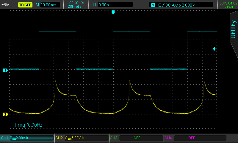
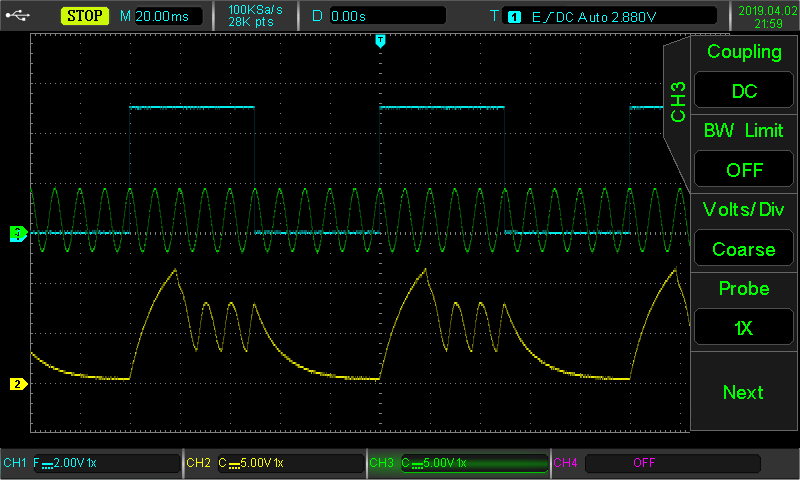
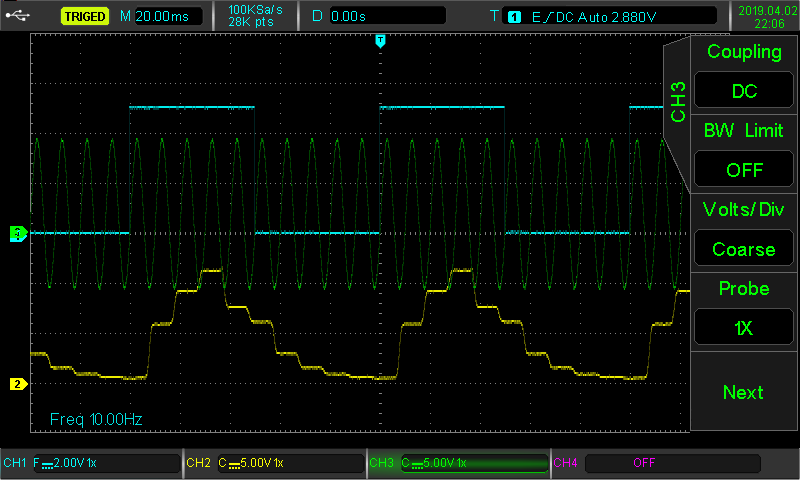
Oscilloscope traces of various envelope waveforms. The blue trace is the gate signal, yellow is the ADSR output, the green trace is a 100Hz sine wave used as a CV source
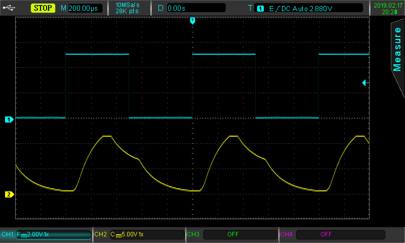
1. A full ADSR cycle over a period of just 1mS with a 1kHz gate signal.
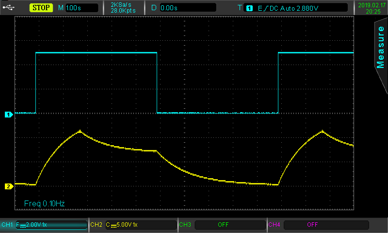
2. With the range switch set to Short, ADSR cycles can last at least 10 seconds with a 0.1Hz gate signal.
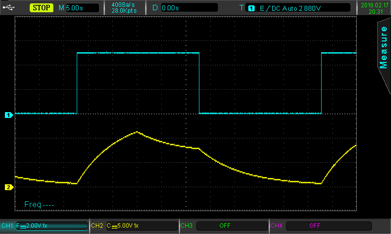
3. With the range switch set to Long, ADSR cycles can last at least 50 seconds with a 0.02Hz gate signal
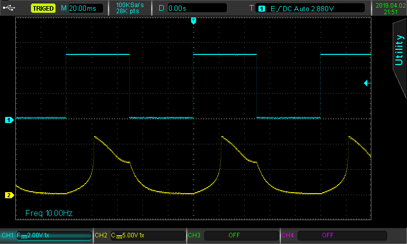
The following traces show the effect of the shape controls and applying a control voltage to the various CV inputs. All use a 10Hz gate signal.
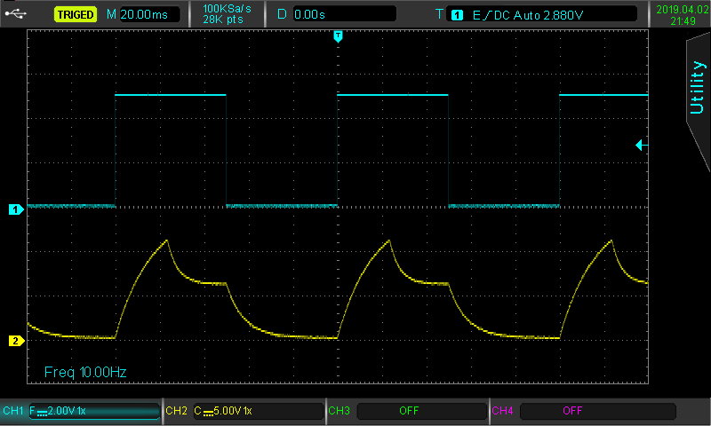
4. A traditional ADSR envelope lasting 100mS
5. The attack shape adjusted, there is an interaction between the shape pots and their corresponding time period. This means adjusting shape also means adjusting time period to keep the same durations
6. Now changing delay shape
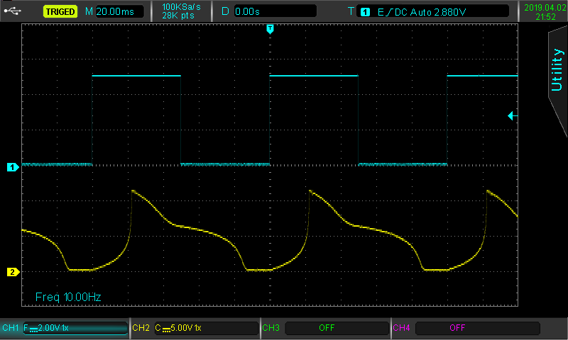
7. Now also changing the release shape
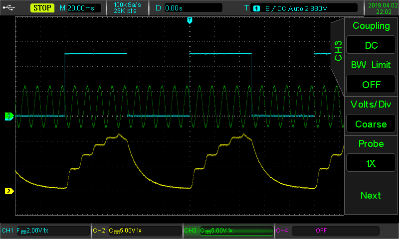
8. Adding a 100Hz sinewave to the attack CV input
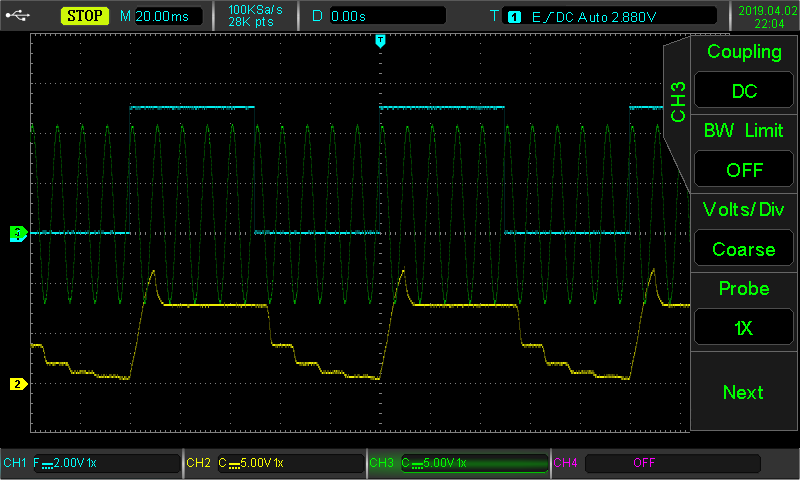
9. Now add the sine wave to the release CV input
10. Now adding the sine wave to the sustain CV input
11. Finally, adding the sine wave to the ADR CV input
This guide is for the construction of the Soundtronics ADSR 3310 in 5U format. Please read through all of the instructions first before commencing as there are some pointers that could make assembly easier.
All parts needed are available from soundtronics.co.uk including:
- PCB: 7215-021
- Electronic components kit: 7215-221
- Front panel: 7215-521
- Back panel: 7215-821
- PCB holder: 7215-921
- PCB fixings: 7210-182
- Angle brackets: 7210-181
- Pot Brackets 7300-000 - 7 off
- Switchcraft jack sockets: 7212-209
- Cliff KM20B knobs: 7210-107
- 3-Way Pot breakout PCB 7210-703
- 4-Way Pot breakout PCB
- Jack sockets breakout PCB: 7210-733
- Your choice of power connector
- Soundtronics 1251-054
- MOTM 7212-305
- Dotcom 7212-302
- Eurorack 7212-301
- JST leads
- 3-way: 7210-103 - 2 off
- 6-way: 7210-106 - 2 off
- 9-way: 7210-109
- 12-way: 7210-112
Not all of the above are absolutely necessary. For example you can hard wire the PCB connections to pots, switches and sockets.
Step 1:
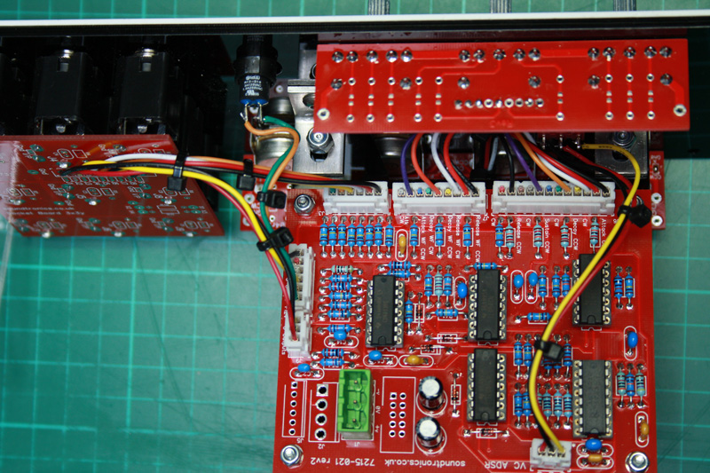
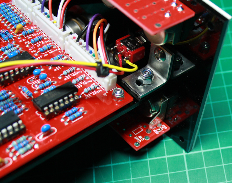
Mount you assembled PCB (7215-021) to the PCB holder (7215-921) using the fixings set (7210-181 and 7210-182). Keep the angle bracket loose at this stage but the 4 PCB fixings can be tightened up, no need to over-tighten otherwise you risk shattering the PCB holder. This photo shows what the finished assembly should look like
Step 2:
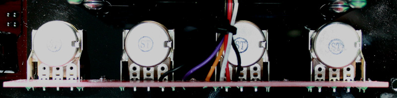
We are using three of our panel breakout PCBs, one for the sockets and two for the pots. Each breakout PCB has optional jumpers that can be soldered across to provide commons. The 4-way ADSR pot PCB 7210-704 requires jumpers A, C, D, E, F, G & H linked. The shape pot PCB 7210-703 requires A, B, C, D, E & F linked. None are required for the socket PCB. Next solder the pots with their pot brackets to the breakout boards ensuring they sit flat on the boards.
Step 3:
Bring the front and back panels together and fit the pots, switches and sockets.
Tips
- Do not use pliers to tighten up the pot, switch and socket nuts as you risk scratching the panel and damaging the zinc plating on the nuts. Use sockets or nut spinners:
- Pots use 10mm
- Toggle switch use 8mm
- Jack sockets use 13mm
- Do not over-tighten the nuts, especially on the pots as it is quite easy to strip their threads
- We do not use washers behind the pot and toggle switch nuts
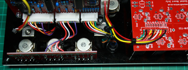
When viewed from the rear, orientate the jack sockets so that the flat corner is to the bottom left, then solder the PCB to the sockets, see photo in step 6. The pot breakout boards are handed as per the photo below. The toggle switch is mounted vertically. You can also fix the PCB holder angle brackets to the back panel using M4x5 screws that came with the brackets.
Step 4:
Wiring can now take place. Many of JST the wires can be cut off which are indicated in the tables below. Starting with the 4-way pot PCB, cut the unused wires off the 12-way JST plug close to the plug. Plug the JST into the corresponding socket on the main PCB. Dress the wires under the PCB holder and trim then solder the wires to the 4-way pot PCB where the unused JST socket outline is shown. Note the pad numbering is from 1 to 12 where 12 is at the bottom of the PCB.
| 1 | Black | 1 (Top pad) |
| 2 | Red | 2 |
| 3 | White | 3 |
| 4 | Yellow | Cut |
| 5 | Orange | 5 |
| 6 | Green | Cut |
| 7 | Blue | Cut |
| 8 | Violet | 8 |
| 9 | Grey | Cut |
| 10 | Brown | Cut |
| 11 | Black | 11 |
| 12 | Red | Cut |
Step 5:
Repeat step 4 but this time for the 3-way pot PCB. This time, the pad numbering on the pot PCB has 9 at the top and 1 at the bottom.
| 1 | Black | 1 (Bottom pad) |
| 2 | Red | 2 |
| 3 | White | 3 |
| 4 | Yellow | Cut |
| 5 | Orange | 5 |
| 6 | Green | Cut |
| 7 | Blue | Cut |
| 8 | Violet | 8 |
| 9 | Grey | Cut (Top pad) |
Step 6:
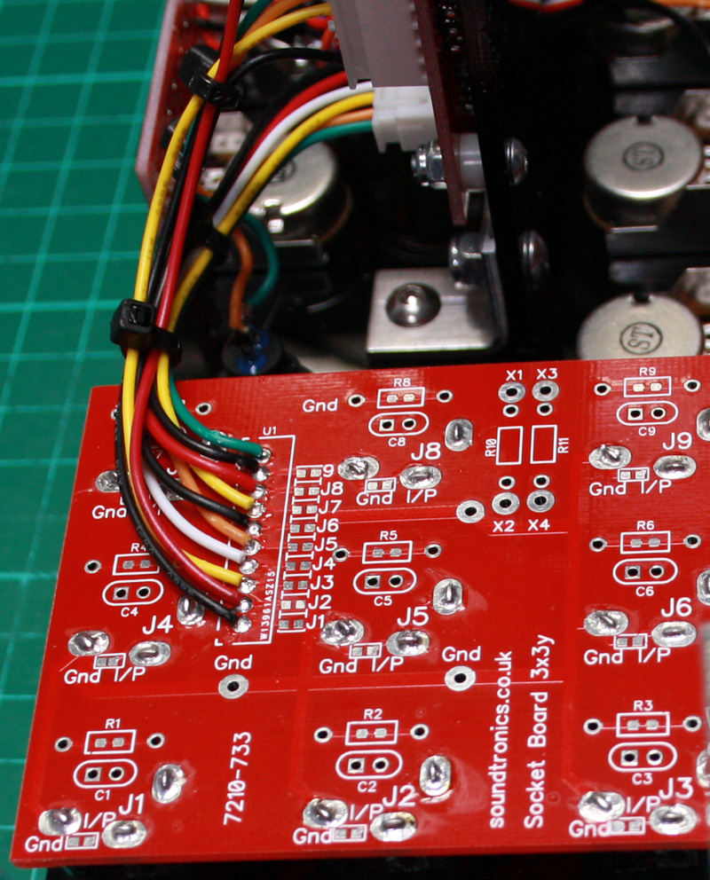
Now plug in the 6-way JST into J3 and solder the wiring to the jack socket PCB as:
| 1 | Black | J9 |
| 2 | Red | J8 |
| 3 | White | J4 |
| 4 | Yellow | J7 |
| 5 | Orange | J5 |
| 6 | Green | Ground which is the pad immediately under the U1 lettering on the PCB |
Step 7:
Now plug in the other 6-way JST into J10 and solder the wiring to the jack socket PCB and push button as:
| 1 | Black | J6 on jack socket PCB |
| 2 | Red | Cut |
| 3 | White | Cut |
| 4 | Yellow | J3 on jack socket PCB |
| 5 | Orange | Push button |
| 6 | Green | Push button |
You can see the push button wiring in the above photo.
Step 8:
That just leaves the two 3-way JSTs, J9 and J8
J9
| 1 | Yellow | Cut |
| 2 | Black | J1 on jack socket PCB |
| 3 | Red | J2 on jack socket PCB |
J8 (Toggle switch)
| 1 | Yellow | Upper contact |
| 2 | Black | Lower contact |
| 3 | Red | Switch common |
For J8, see the photo in step 3 for wiring to the toggle switch.
Assembly has now been completed and you can proceed to testing. Before inserting the chips, power up the board first and double check supply polarity on the socket for U1 (TL084). With respect to ground 0V, pin 4 is +12V and pin 7 is -12V or +/-15V if that is your power supply voltage.
After removing power, proceed with plugging in the chips ensuring correct orientation. As there is no setting up, you are ready to go and test its operation.
How it works:
Much of the hard work is carried out by the AS3310 ADSR chip. The attack, decay and release periods are set by applying a voltage of between 0 and -240mV to the respective pins which is derived from the inverting summating amplifiers in U1. Each ADR time period pot wiper is applied to the inverting amplifiers via a 120k resistor (150k for +/-15V operation) to give a gain of 0.833 (0.666 +/-15V) so the amplifier output gives 0 to -10V range for full pot travel. The amplifier outputs are applied to a voltage divider to take the -10V down to -240mV. Three additional inputs to each of these summating amplifiers are provided, one for external CV for the ADR periods (via R10, R9, R8), one for a common ADR CV (via R6, R5, R6), and one for the shape (R24, R22, R23).
The sustain input to the AS3310 is similar but requires a 0 to +5V signal to give a 0-100% of the peak attack voltage. Once again this is achieved using a summating inverting amplifier U1.3 which is immediately inverted again by a unity inverting amplifier U3.1 as the ADSR requires a positive going voltage for sustain control unlike the ADR time periods. U1.3 has a gain of 0.425 (0.34 +/-15V) to give the 5V sustain control.
The AS3310 requires a bipolar supply but the negative supply to Vee is limited to 7V whereas the positive supply Vcc can go to 18V. R22 is used to set the Vee supply which is calculated using the formula:
R22=(supply voltage -7.5)/0.01
For 12V, this gives 450R, nearest preferred value being 470R. For 15V, it is 750R.
The shape control of the ADR envelopes uses a feedback loop between the ADSR output and the corresponding ADR CV inputs. The amount of feedback and hence the shape is determined by the shape waveforms potentiometers. The greater the voltage, the more logarithmic the shape but as the attack shape is already logarithmic, it is inverted by U3.2 so an increasing voltage from the attack waveform pot makes the shape more exponential. There is an interaction between the ADR timing periods and the amount of shape voltage applied. As you modify the shape, you will need to compensate for the timing period changes using the main ADR pots.
The AS3310 requires both a gate pulse and a trigger pulse simultaneously to start the ADSR cycle. Fortunately, we can create the trigger pulse from the gate pulse using a capacitor - C7. The gate pulse can come from either the manual pushbutton or the gate socket. The pushbutton has a CR contact debounce before joining with the gate socket input at U5.1 non-inverting input. U5.1 is a comparator that quickly flips its output from negative to positive saturation when the non-inverting input (pin 3) voltage exceeds 2V (for 12V operation or 2.5V for 15V operation). The threshold is set by R45 & R44 at the inverting input (pin 2). The comparator output is fed to the AS3310 gate input via D5 to ensure the AS3310 only sees positive voltages. Unlike our simpler ADSR 3310, this model also has a trigger function that will create a full AR envelope with just a brief 1mS pulse. The brief trigger pulse is latched by U4.1 which creates the Gate signal the AS3310 requires but this latch is reset at the end of the attack phase (from U3.4) so the AS3310 immediately starts the release phase.
The ADSR envelope output from the AS3310 is buffered by U5.3 and U5.2 before feeding the output sockets via R36 and R54.
There is a risk that the sustain voltage could exceed the peak attack voltage giving undesirable results. Pin 3 of the AS3310 outputs the peak attack voltage which is connected to a precision peak follower U5.4 which is connected to the sustain voltage input of AS3310 pin 9 to prevent this situation.