


YuSynth Triple Clock Divider
Introduction
A bare double sided PCB (no need for the wire jumper links shown on the PCB layout) for the Yusynth Triple Clock Divider synth module. These PCBs are manufactured by Soundtronics with a percentage of the sale going to the creator of the YuSynth - Yves Usson. These are early days for the YuSynth Modular Synth at Soundtronics, our plan is to stock PCBs for all of the projects as well as components, kits and front panels. This is going to take time but will eventually be as comprehensive as our MFOS range.
No components are included with the PCB but check out our Synth Components section where you should find what you need. We do suggest visiting the YuSynth Clock Divider project page for detailed information on both this PCB and the accompanying VC-Panner including Yves panel layouts but a summary is shown below.
Erratum
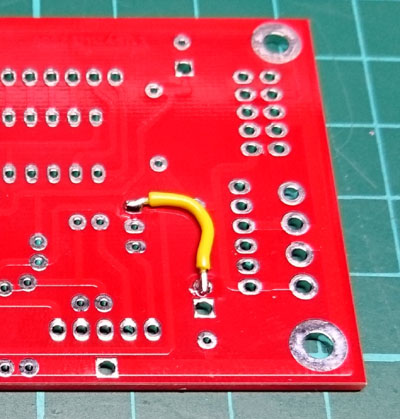
Sorry but there is small error on the PCB. A track is missing between the junction of C1 / R1 and +VLED. Our thanks to Flareless on the muff wiggler forum for identifying not only the problem but also the solution.
After soldering in components C1, R1 and Q9, solder an insulated wire link between the junction of C1 / R1 and the collector of Q9 as shown below.
Description
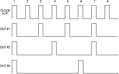
This module is meant to be a complement of step sequencers or to be used to trigger events at regular beats. It provides a way of clocking up to three step sequencers at various rates from a single external master clock, the master clock rate can be divided by 1 (unchanged rate), 2, 3, 4, 5, 6, 7 or 8 independently on the three dividers.
The three dividers can be clocked by the same clock signal on input IN #1, but a different master clock can be used for the second and third dividers by plugging it in the input IN #2 & 3.
The divided clock signals are available at outputs OUT #1, OUT #2 and OUT #3, and are visualized with LEDs.
A RESET input is provided to synchronize the dividers. Note that the outputs are all shaped to the same pulse width as that of the external clock.
Example : one master clock, STEP #1 = 1/2, STEP #2 = 1/3, SETP #3 = 1/5
The PCB can accept a choice of three types of power connector, it can be either a Synthesizers.com 6 pins MTA connector, a MOTM 4 pins MTA96 connector or a 10-pin Eurorack connector.
Circuit
Channel #1:
The input signal is applied to a Schmitt trigger (Q1-Q2) which converts the clock signals to a proper logical level (0V or 15V). Q1-Q2 are connected as a classical discrete Schmitt trigger. R3,R4 are large value resistors that insure a high input impedance. Diode D1 prevents the input transistor from negative voltages. The logical level available at the collector of Q1 is applied to the CLOCK pin (pin 14) of a classical decade counter CMOS IC (4017). The 0 count pin of the 4017 (pin 3) is sent to one input (D5) of a discrete AND gate formed by D4, D5 and R9. The second input (D4) of this AND gate receives the clock signal from the collector of Q2. This way the output is shaped to the same pulse width as the clock input. Q3 acts as a buffer and the output signal is available through R17. LD1 show the status of the output. With the values shown on the schematics the logical ON level is 10V. If a 5V level is preferred, then use the optional zener diode Z1 (5.1V), the PCB is provided with pads for soldering the optional zener. The other counting pins of the 4017 (1 to 8) are sent to a eight position rotary switch which common pin is connected to one input (D3) of a discrete OR gate formed by D2, D3 and R8. This OR gate is connected to the RESET pin (pin 15) of the 4017 and resets the decade counter to 0 when the number of steps selected with the rorary switch has been reached. The second input (D2) of the OR gate is connected to a sub-circuit built with Q10 and Q11. This sub-circuit makes it possible to reset the counter to 0 with an external RESET signal. The external reset signal is applied to the base of Q10. The capacitor C10, differentiates the logical level at the collector of Q10 and the positive part of the differentiated signal is converted to a 1 ms pulse by Q11. Then this pulse is sent to D2.
The maximum current draw of this module is 20mA at +15V.
Click on the schematic thumbnail above for the circuit diagram.
Wiring
The wiring schematic image in the above thumbnails show the panel wiring to the pots and sockets etc.
Setting and Trimming
This circuit requires no setting or trimming. It must work right away.
Parts List
The parts list below is direct from the YuSynth website. The value in the parts list is the default value and may differ to that quoted in the schematic / PCB silk image.
The parts list excludes knobs although we have standardised on the Cliff KM20B but it does include 1/4" jack sockets. All parts are available individually (use the part number in the search box above) or as a components kit that excludes sockets and knobs.
| Reference | Value | Part No. | Qty |
| U1,U2,U3 | 4017 CMOS decade counter | 7212-510 | 3 |
| Q1.....Q11 | BC547 | 7212-401 | 11 |
| D1.....D16 | 1N4148 | 7212-480 | 16 |
| Z1....Z3 | optional 5V zener diodes (see text) | 2101-502 | 3 |
| R1,R2 | 10 ohm 5% | 7163-007 | 2 |
| R5,R12,R17,R24,R29,R36 | 220 ohm 5% | 7163-035 | 6 |
| R8,R14,R20,R26,R32,R38 | 1K 5% | 7163-051 | 6 |
| R13,R25,R37 | 1.5K 5% | 7163-055 | 3 |
| R10,R22,R34 | 4.7K 5% | 7163-067 | 3 |
| R41 | 10K 5% | 7163-075 | 1 |
| R6,R7,R9,R18,R19,R21,R30,R31,R33,R42 R43 |
22K 5% | 7163-083 | 11 |
| R39 | 100K 5% | 7163-099 | 1 |
| R11,R23,R35 | 220K 5% | 7163-107 | 3 |
| R3,R15,R27,R40 | 1M 5% | 7163-122 | 4 |
| R4,R16,R28 | 1.2M 5% | 7163-128 | 3 |
| C6 | 1nF to 2.2nF polyester film | 7212-708 | 1 |
| C3,C4,C5 | 100nF multilayer ceramic | 7212-749 | 3 |
| C1,C2 | 22µF/25V electro. | 7213-108 | 2 |
| LD1,LD2,LD3 | Panel Mount | 7213-900 | |
| LD1,LD2,LD3 | Red LED | 7213-901 | 3 |
| Jk1...Jk6 | 6.5 mm jack socket | 7212-206 | 6 |